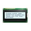
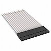
| Enclosure |
33.05
|
| Tilt Stand |
1.37
|
| Gasket |
1.60
|
| Banana |
1.82
|
| Banana |
1.82
|
| Mono Jack |
2.14
|
| USB CONN |
9.54
|
| Charger Jack |
6.49
|
| Display |
25.82
|
| Flex Cable |
16.34
|
| Total |
99.99
|
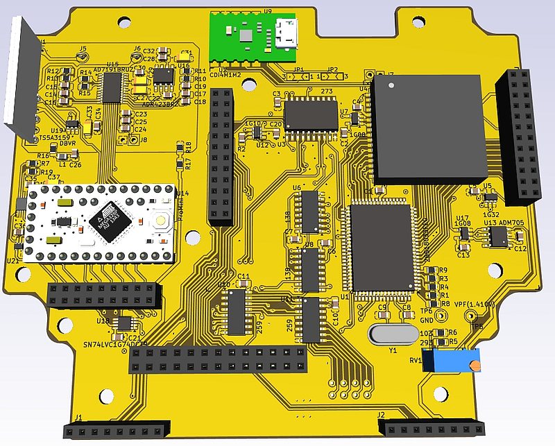
- The Main Board is a four-layer design, there are no parts on the bottom
- White microcontroller board middle-left is Sparkfun Pro Mini, its job is to read the ADC and pass the numbers to the CPU. The microcontroller also reads a temperature sensor inside the ADC and attempts to set the LCD contrast through a digital potentiometer. Small green board at top is FTDI UMFT234XF, this little board is the USB to serial function translator.
- The square thick chip top right is the DS1553 RTC, the 3D model used here is not an exact representation of the chip and battery assembly, but it is accurate dimensionally. The two pieces are: Bottom piece with all the circuitry and top piece with lithium battery and crystal
- There are 210 parts across all 5 boards, there are upwards of 1,200 solder joints. The boardset tally for all parts, excuding decals and display window, is just under $1,000 CDN
- All images below have associated image maps, hover the mouse pointer over a part of interest and when the pointer changes you have the option of a direct link to the part supplier, in most cases, Digikey
| Price snapshots captured 2025/10/06 | ||||
| Q |
Description
|
Digikey
|
Each
|
Total
|
| 1 | U9 - USB to serial converter |
10.91
|
10.91
|
|
| 1 | U4 - DS1554 RTC |
74.41
|
74.41
|
|
| 1 | U4 - RTC Battery Module |
23.09
|
23.09
|
|
| 1 | U14 - Pro Mini Arduino board |
17.10
|
17.10
|
|
| 1 | U1 - S180 33MHz |
36.17
|
36.17
|
|
| 1 | U15 - ±24-bit ADC, AD7191BRUZ |
21.87
|
21.87
|
|
| 1 | U16 - 3V Ref., ADR423BRZ |
22.50
|
22.50
|
|
| 1 | U13 - ADM705ARZ Supervisor |
7.63
|
7.63
|
|
| 1 | U18 - 1G74 SN74LVC1G74DCTR |
0.89
|
0.89
|
|
| 1 | U5 - 1G32 1G32DBVR, SOT23-5 |
0.16
|
0.16
|
|
| 2 | U7, U17 - 1G08DBVR, SOT23-5 |
0.16
|
0.32
|
|
| 1 | U12 - LVC1G10DBVR, SOT23-6 |
0.36
|
0.36
|
|
| 1 | U19 - TS5A3159DBVR -Switch |
0.87
|
0.87
|
|
| 1 | U21 - OpAmp AD8565AKSZ, SC70 |
4.88
|
4.88
|
|
| 1 | U20 Digital Pot, AD5259BRMZ10 |
7.21
|
7.21
|
|
| 1 | U3 - 74LVC273, 20 SOIC |
0.81
|
0.81
|
|
| 2 | U6,U8 74HC138D Toshiba SO16 |
0.57
|
1.14
|
|
| 2 | U11, U20 74HC259D Toshiba SO16 |
0.57
|
1.14
|
|
| 1 | RN1 - Caddock decade divider |
60.67
|
60.67
|
|
| 21 | C1,C2,C3,C4,C5,C6,C7,C10,C11, C12,C13,C20,C21,C22,C26,C28, C30,C32,C34,C35,C36 0.1uF, 0805 |
0.07
|
1.47
|
|
| 2 | C8, C9 Oscillator caps 22pF, 0805 |
0.15
|
0.30
|
|
| 5 | C27,C29,C31,C33,C37 10uF, 1206 |
0.63
|
3.15
|
|
| 6 | C15,C16,C18,C19,C23,C25 10n |
0.12
|
0.72
|
|
| 3 | C14,C17,C24 1uF, 50V, 0805 |
0.12
|
0.36
|
|
| 7 | R1,R3,R4,R8,R9,R14,R15 104 0805 |
0.26
|
1.82
|
|
| 4 | R10,R11,R12,R13n 100R 0805 |
0.26
|
1.04
|
|
| 1 | R2 - 1K |
0.17
|
0.17
|
|
| 1 | R5 - 29.4K |
0.16
|
0.16
|
|
| 3 | R6, R7, R19 10K |
0.23
|
0.69
|
|
| 1 | R16 - 1R5 |
0.16
|
0.16
|
|
| 1 | R17 - 10M MCA1206MD1005BP500 |
0.37
|
0.37
|
|
| 1 | R18 - 1.111M RT1206BRE071M111L |
0.45
|
0.45
|
|
| 1 | RV1 - 10K Pot 3296W |
5.95
|
5.95
|
|
| 1 | Y1 - Crystal HC49/U, 7.372800MHz |
0.79
|
0.79
|
|
| 1 | J1, J2 Conn_01x08 Female |
1.99
|
3.98
|
|
| 1 | J3 - Conn_02x13_Female |
8.27
|
8.27
|
|
| 1 | L1 - Choke, 1K@100MHz |
0.19
|
0.19
|
|
| 1 | Large PCB |
20.00
|
||
|
Total
|
341.98
|
|||
| Q |
Description
|
Digikey
|
Each
|
Total
|
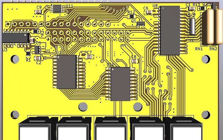
| 1 | U1 - LVC1G125DBVR, SOT23-5 |
0.19
|
0.19
|
|
| 2 | U2, U10 - 74HC645DWR |
2.40
|
4.80
|
|
| 1 | U3 - 74HC112 |
1.88
|
1.88
|
|
| 1 | U8 - Keyboard Encoder |
7.50
|
7.50
|
|
| 1 | U11 - 74LVC1G74 |
0.89
|
0.89
|
|
| 1 | Q1 - BSS138 SOT23-3 |
0.28
|
0.28
|
|
| 1 | Q2 - MMBT3904 SOT23-3 |
0.11
|
0.11
|
|
| 6 | C1,C5,C6,C7,C8,C9 |
0.10
|
0.60
|
|
| 1 | C2 - 300pF |
0.31
|
0.31
|
|
| 2 | R1, R2 - 2K2 0805 |
0.16
|
0.32
|
|
| 1 | R12 - 47R 0805 |
0.10
|
0.10
|
|
| 1 | R13 - 1K 0805 |
0.11
|
0.11
|
|
| 2 | RN1, RN2 4K7 |
0.28
|
0.56
|
|
| 1 | Y1 - 4MHz Crystal |
0.84
|
0.84
|
|
| 1 | PCB |
20.00
|
20.00
|
|
|
Total:
|
38.49
|
| Q |
Description
|
Digikey
|
Each
|
Total
|
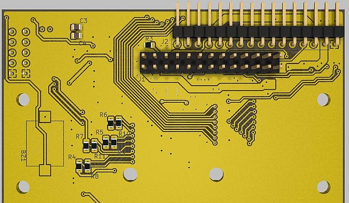
| 1 | J1 |
1.46
|
1.46
|
|
| 1 | J2 |
0.97
|
0.97
|
|
| 1 | R3 - 100K, 0805 | RC0805FR-7W100KL |
0.14
|
0.14
|
| 2 | C3,C4 - 18pF | C0805C180J5HACTU |
0.10
|
0.20
|
| 8 | R4,R5,R6,R7,R8,R9,R10,R11 |
0.14
|
1.12
|
|
| 5 | Grayhill single key |
15.76
|
78.80
|
|
| 2 | Grayhill 1x3 keys |
28.27
|
56.54
|
|
| 2 | Grayhill 3x4 key matrix |
66.29
|
132.58
|
|
|
Total:
|
271.81
|
|
Q
|
Description
|
Man. Part # Digikey
|
Each
|
Total
|
|
2
|
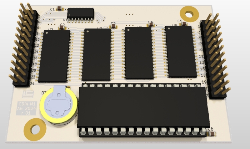
J1 - J2, CONN HEADER VERT 24POS .1" | 61302421121 |
2.16
|
4.32
|
| Mating WR-PHD 2.54 MM DUAL SOCKET | 61302421821 | |||
| CONN HDR 24POS 0.1 GOLD PCB | PPPC122LFBN-RC | |||
|
4
|
U2 - U5, IC SRAM 4MBIT 32TSOP II | AS6C4008-55ZIN |
8.73
|
34.92
|
|
1
|
U1, IC X4 SRAM NONVOL CTRLR 16-SOIC | BQ2204ASN-N |
-
|
14.13
|
|
1
|
BT1, BATTERY LITHIUM 3V COIN 12.5MM | BR-1225/HCN |
1.68
|
1.68
|
|
1
|
CONN IC DIP SOCKET 32POS GOLD | 115-43-632-41-003000 |
7.69
|
6.60
|
|
1
|
U6, EEPROM AT29C512 FROM STOCK |
Check Prices Today!
|
5.00
|
5.00
|
|
6
|
C1 - C6, CAP CER 0.1UF 50V X7R 0805 | 0805B104J500CT |
0.15
|
0.90
|
|
1
|
Small PCB |
10.00
|
10.00
|
|
|
Total:
|
78.64
|
|||
| Price snapshots captured 2025/Oct/09 | ||||
| Q |
Description
|
Digikey
|
Each
|
Total
|
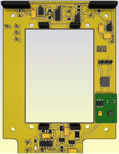
| 1 | U1 - ICL7663ACSA+ 8 SOIC |
9.98
|
9.98
|
|
| 1 | U2 - MAX667CSA+ 8 SOIC |
12.70
|
12.70
|
|
| 1 | U3 - CD4013BM96 14 SOIC |
0.75
|
0.75
|
|
| 1 | U4 - ICL7662EBA+T 8 SOIC |
12.43
|
12.43
|
|
| 1 | U6 - 78L05 SOT89 |
0.26
|
0.26
|
|
| 1 | U7 - Preregulator PCB |
2.99
|
2.99
|
|
| 1 | U8 - MAX712ESE+ |
19.60
|
19.60
|
|
| 1 | Q1 - PBSS5350X,135 |
0.71
|
0.71
|
|
| 2 | D1, D2 - 1N4148 |
0.52
|
1.04
|
|
| 1 | D3 - Bridge MRS30M |
0.65
|
0.65
|
|
| 1 | D4 - Blue LED 1206 |
0.37
|
0.37
|
|
| 1 | D5 - 30V, 5A SOD128 |
0.96
|
0.96
|
|
| 2 | R1, R6 - 10K 1206 |
0.16
|
0.32
|
|
| 1 | R2 - 68Ohm 1206 |
0.16
|
0.16
|
|
| 1 | R3 - 909K 1206 |
0.16
|
0.16
|
|
| 1 | R4 - 680K 1206 |
0.16
|
0.16
|
|
| 1 | R5 - 1.2M 1206 |
0.16
|
0.16
|
|
| 1 | R7 - 4.7K 1206 |
0.16
|
0.16
|
|
| 1 | R8 - 68K 1206 |
0.16
|
0.16
|
|
| 1 | R9 - 22K 1206 |
0.16
|
0.16
|
|
| 1 | R10 - 150Ohm 1206 |
0.16
|
0.16
|
|
| 1 | R11 - Current Sense 2512 0.25Ohm |
0.89
|
0.89
|
|
| 5 | C1,C2,C3,C6,C7 104 1206 |
0.12
|
0.60
|
|
| 1 | C4 - 225 |
0.67
|
0.67
|
|
| 1 | C5 107 6032 | T495C107K016ATE200 |
2.64
|
2.64
|
| 4 | C8,C9,C10,C14 106 6032 |
1.08
|
4.32
|
|
| 2 | C12,C13 103 10n 1206 |
0.68
|
1.36
|
|
| 1 | C11- 225 6032 |
0.96
|
0.96
|
|
| 2 | J1, J2 Conn_01x08 Female |
1.99
|
3.98
|
|
| 4 | J3,J4,J5,J6 Conn_01x03 Female |
1.05
|
4.20
|
|
| 1 | J7 3 POS Header |
0.87
|
0.87
|
|
| 1 | J7 3 POS Terminal Block |
2.46
|
2.46
|
|
| 1 | Small PCB |
10.00
|
10.00
|
|
|
Total:
|
93.66
|
|||
|
Q
|
Description
|
Man. Part # Digikey
|
Each
|
Total
|
|
5
|
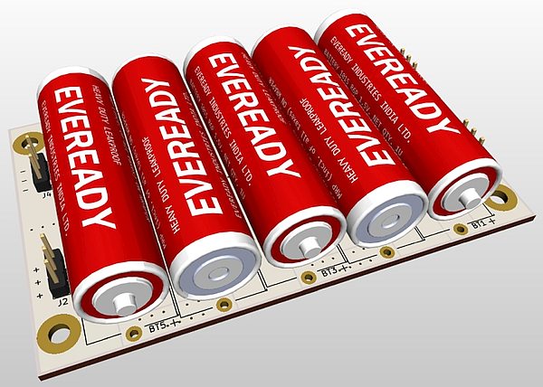
BT1-BT5, AccuLoop-X 2600mAh AA cell |
6.30
|
31.50
|
|
|
4
|
J1 - J4, CONN HEADER VERT 3POS .1" |
0.19
|
0.96
|
|
|
1
|
Small PCB |
10.00
|
10.00
|
|
|
Total:
|
42.46
|
|||
The QFP package (local picture) is a Surface-Mounted Device, SMD, so it must be soldered directly to the PCB traces, the PLCC package (local picture) of the chip is also an SMD but this one can optionally be socketed in which case we are likely to have a problem because the socket's height is over 1/4" and this might make it difficult to fit the flipped memory board right over it. We will most likely select the QFP version, the whole assembly is moving from through-hole to SMT.
 |
||
The 2000 ICISS had a 6.144MHz crystal in it but its clock rate was only half of that due to a programmable divide by two flip-flop inside the chip. The recent modifications and upgrades brought about the usage of a 7.3MHz crystal and this resulted in a unit with both low and high speeds, namely, 7.3MHz or 3.65MHz. The 7.3MHz mode results in a maximum baud rate of 115.2K, if we were to increase the clock rate four-fold we would also increase the baud rate four times to about 460.8K bits per second, roughly 46K bytes per second, so a binary download of all storage memory would take 25 seconds or so. If we double the storage memory to 2 MB we can still dump all that in binary mode in less than a minute. Some serious testing to be done here, how much do we increase the clock rate, do we double it, triple it, quadruple it, and does the increase affect reliability, and if so, how? The 20MHz version of the DIP mentioned above was used in a test unit, operation at 14.6MHz has been verified with no issues.
A minimum of 5 PCBs must be designed no matter what, a Main Board PCB (1), two Memory Board PCBs (2) already done see below, a Power/Charging Board PCB (1) and a Keyboard PCB (1). It is likely that a sixth PCB will be needed to house the analogue circuitry with the ADC and the microcontroller, see the ADC section below.
So the job description is:
- Double, triple, or quadruple the clock rate from 7.3MHz to 14.6MHz, 21.9MHz, or 29.2MHz
- Double the storage memory from 1MB to 2 MB
- Potentially double the EEPROM size from 64K x 8 to 128K x 8
- Get rid of the lead-acid battery/charging, replace it with NiMH which will instantly more than double capacity
- Make the move from ±15-bits ADC to ±23-bits ADC and offload the job, min/max, qsort, etc. to a microcontroller, automate calibration
- Get rid of that ancient keyboard encoder already!
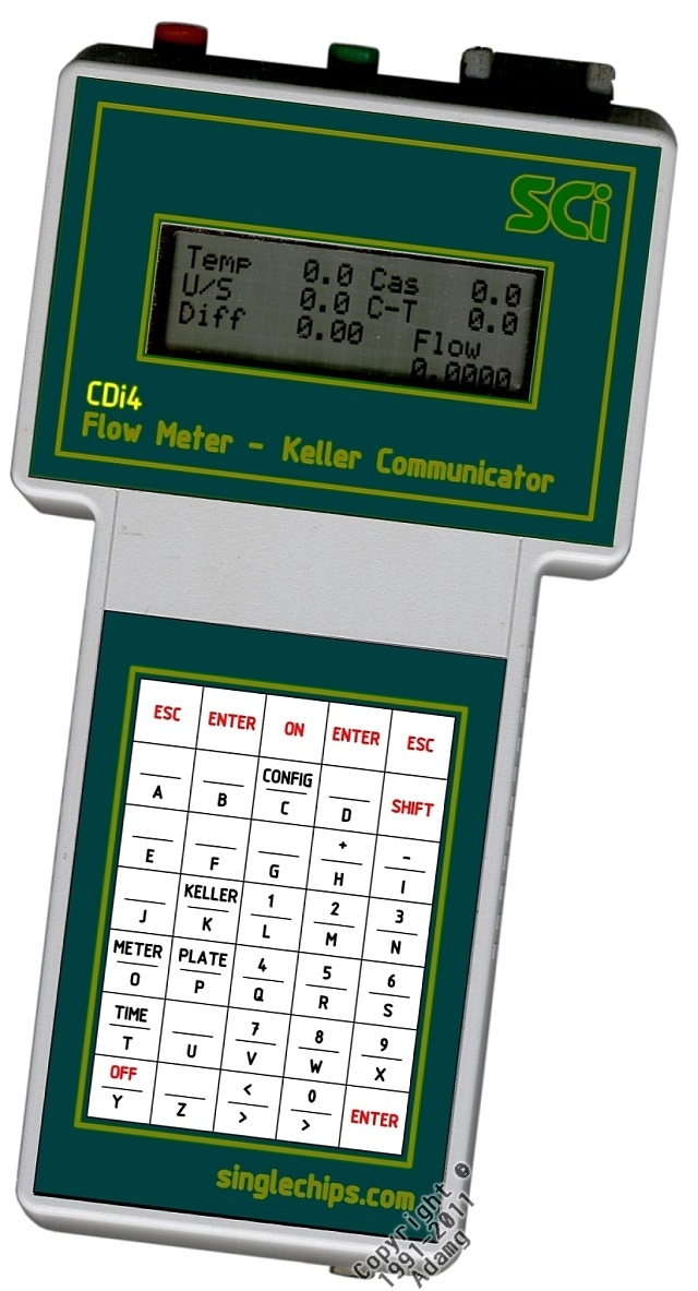
- Get rid of that DB9 serial connector at unit front, include USB to serial circuitry within unit, outside only needs USB connector
- Board status: designed June 2016, not built yet.
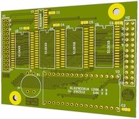
- Doubles the ICISS1/CDi3 storage Static RAM, SRAM, to 2 Mbytes.
- Accommodates 64k x 8 and 128k x 8 EEPROMS in 32-pin DIP packages.
- Board pdf: layers combined, board pdf: layers on separate pages.
- Board status: designed June 2016, not built yet.
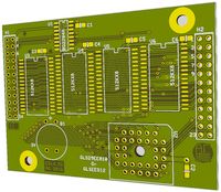
- Doubles the ICISS1/CDi3 storage Static RAM, SRAM, to 2 Mbytes.
- Accommodates 64k x 8 and 128k x 8 EEPROMS in PLCC packages.
- Board pdf: layers combined, board pdf: layers on separate pages.
 Very small USB to serial converters can now be purchased, we should include one inside the unit, so we only need a suitable connector and a standard USB patch cord. Example connector to replace the DB9 serial connector in the picture on the left, click for larger image.
